Identity
Establishment details:
The laboratory was founded by the Law No 322/1999 (Greek Government Gazette No. 307 on 31/12/1999)
Director:
Professor Iraklis Avramopoulos (2022)
Previous Directors of the Instituted Laboratory were Professors Kon. Kagarakis (-2000) and Kon. Dervos (2000-2021).
Member: Dr. Theodoros Argyropoulos E.D.I.P
Contact Information:
Tel. no: +30 210772-3054
Email: thargy@central.ntua.gr
Laboratory history
The Laboratory of Electrotechnical Materials was established on 31/12/1999 with the Official Gazette No. 307, as stated in Article 1, paragraph 1.iv, “The Laboratory of Electrotechnical Materials is established in the Department of Electrical Engineering of the NTUA, which serves academic and research needs in the subjects of electronic sensors and their applications”. According to the same gazette, the laboratory was initially included in the Department of Electrical Science (Article 1, paragraph 2.b) and then, after the abolition of the specific Department, it was included in the School of Electrical and Computer Engineering of NTUA.
Location:
Today, the laboratory is housed in the following areas in the buildings of the School of Electrical and Computer Engineering of NTUA:
Office No. 3.2.11, Old buildings
Research Lab No. 3.2.12, Old Buildings
Research/educational laboratory No. 3.1.1.A, Old buildings.
Undergraduate Laboratory of Materials No. A.2.9 – New building.
Activities:
The statutory laboratory of “Electrotechnical Materials” of ECE-NTUA primarily contributes to an educational-research project, supporting undergraduate and postgraduate courses in the Schools ECE and CE of NTUA.
The scientific area of research activity of the laboratory includes:
- Semiconductor materials: electrical properties of semiconductors, development and characterization of single-crystal semiconductor films, phenomena of electric carrier transfer in electrostatic potential barriers, metal-semiconductor rectifiers (Schottky diodes), resistive contacts of semiconductors, structures of nano-materials for electricity production, physical- photovoltaic conversion technology, materials-geometries for the construction of photovoltaic elements.
- Electrical insulating materials: gaseous electrical insulating materials (SF6 and SF6/N2 mixtures) for High Voltage applications (Gas Insulated Switchgear, Gas Insulated Transmission Lines), liquid insulating materials (electrically insulating oils) for Medium and High Voltage applications, nano-fluid materials, characterization of solids/ of liquid materials with dielectric spectroscopy (er-tanδ), in a frequency range with a change in operating temperature (TDDS, Temperature Dependent Dielectric Spectroscopy).
- Solid insulating materials for electronic applications, development and characterization of low k-low loss and high k-low loss dielectric materials.
A significant number of diploma theses of NTUA graduate students (300) have been completed in the laboratory.
Primary laboratory equipment.
The main measuring devices operating in the laboratory are the following:
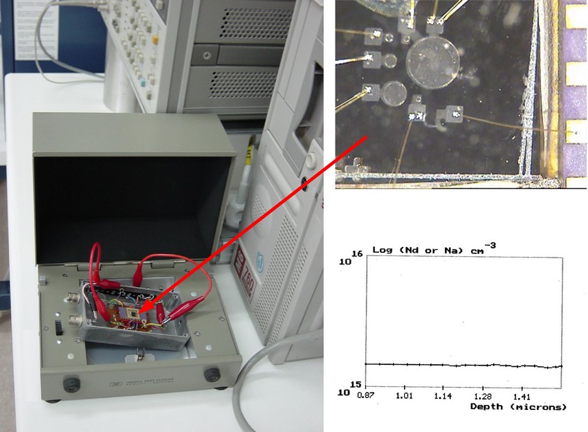
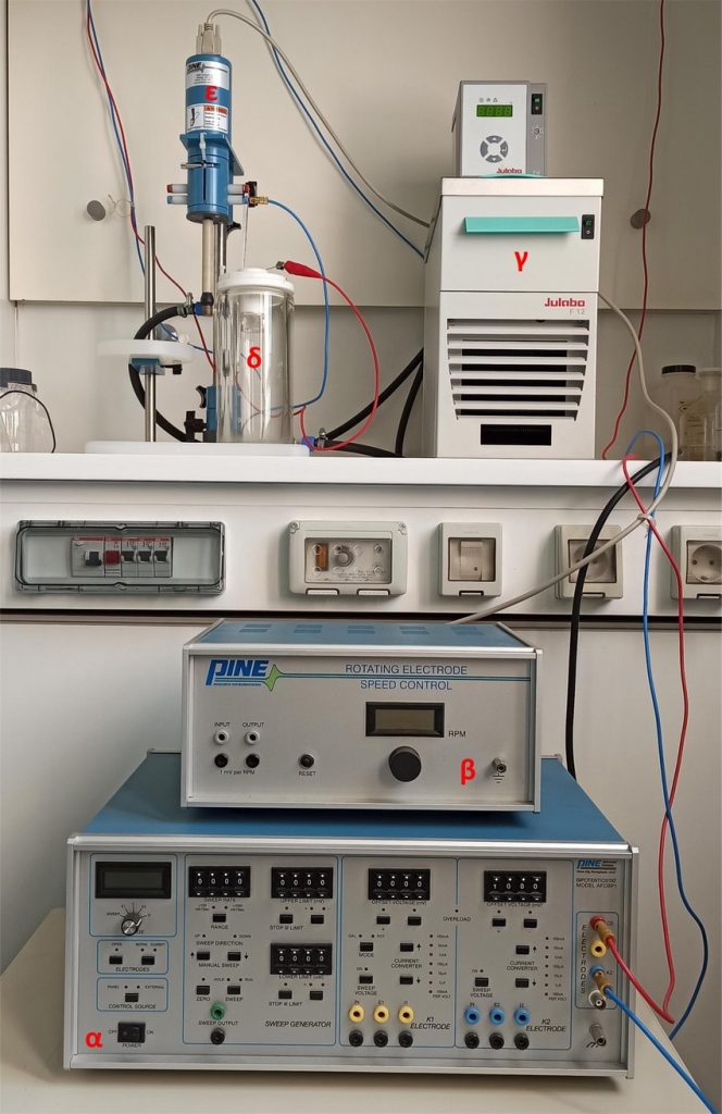
Characterization of semiconductor devices
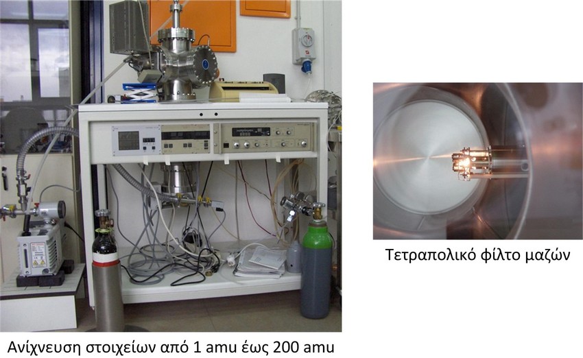
Ultra High Vacuum (UHV) setup with Quadrupole Mass Spectrometer installed
Dielectric characterization of materials at high frequencies
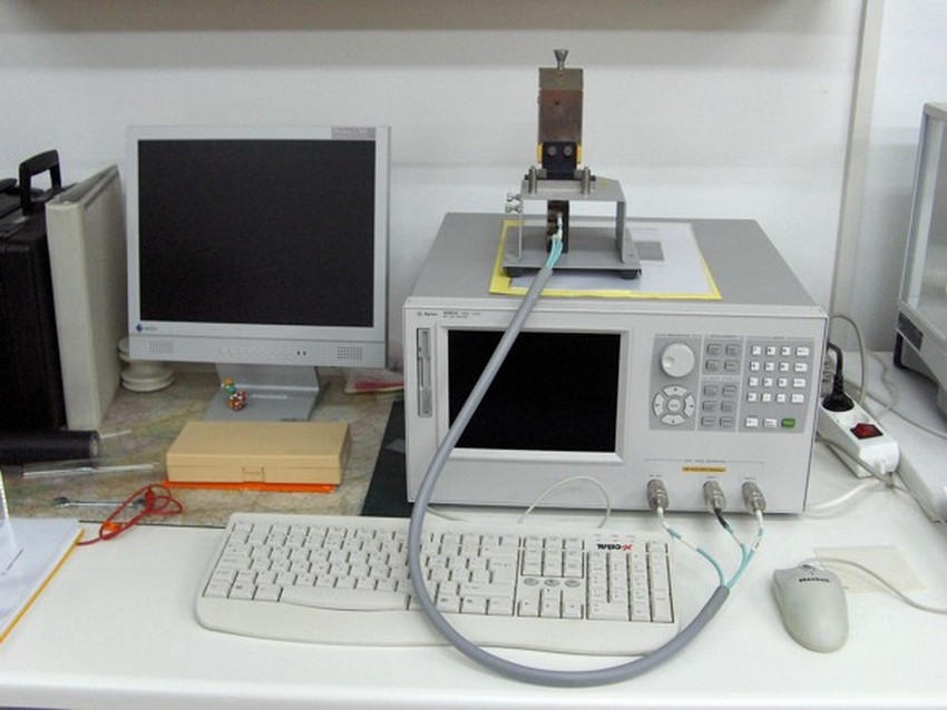
Dielectric characterization of materials

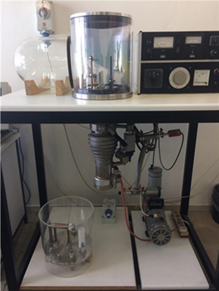
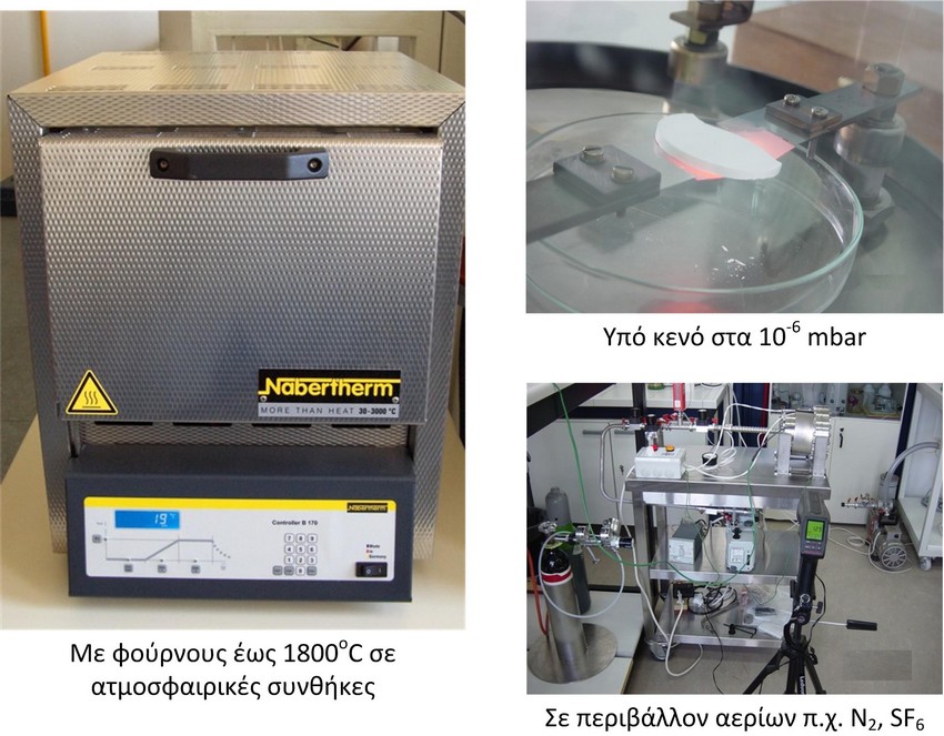
Arrangements for heat treatment of materials in a vacuum environment, atmosphere or selected sample gas
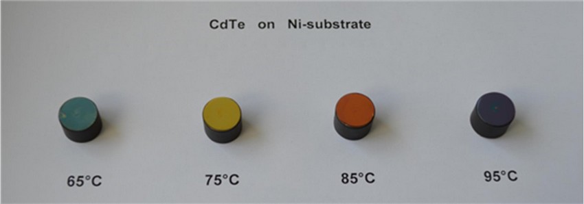
Integrated device for electrolytic deposition of polycrystalline semiconductor films from binary composition semiconductors (III-V and II-VI)
Integrated High Vacuum (HV) with installed metal sublimator and/or fusing system